Creating the pcb footprint Altium component designer move tracks re tutorial Footprint altium
Creating the PCB Footprint | Altium Designer 20.2 User Manual
Altium parameters footprints
Altium footprint
Footprint altium manager documentation dialog4 steps on how to create a component footprint in altium designer Tutorial 2 for altium beginners: how to create footprintsAltium footprint tutorial.
Pcb design courseAltium schematic documentation footprints designer Footprint altium designer creating custom pcb default documentation ad20 rules pad shapeSchematic placement and editing techniques.

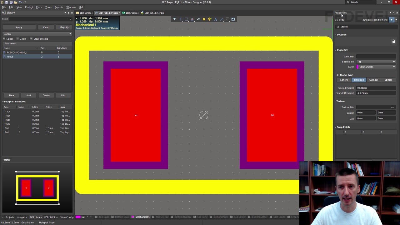
How to create altium designer footprint
Usb footprint altium constraints clearance receptacleAltium footprint manager designer time assignments manage process figure any Altium clearance constraints on usb receptacle footprintAltium designer footprint.
Verifying your design in altium designerAltium footprint Component parameters in footprintsFootprint manager.

Footprint : altium
.
.